 Newshot
skills/bom/SKILL.md · 78 lines · 6.2 KB
description: Resolve and review exact PCB parts, packages, electrical ratings, availability, and manufacturer BOM fields for KiCad projects.
skills/export/SKILL.md · 120 lines · 4.6 KB
description: Generate deterministic KiCad ERC, DRC, fabrication, assembly, documentation, and 3D export outputs with kicad-cli.
- kicad-cli version
- kicad-cli sch erc
- kicad-cli pcb drc
- kicad-cli sch export pdf
- kicad-cli sch export bom
- kicad-cli sch export netlist
- kicad-cli pcb export gerbers
- kicad-cli pcb export drill
- kicad-cli pcb export pos
- kicad-cli pcb export pdf
- kicad-cli pcb export step
- kicad-cli pcb render
- references/kicad_cli_command_fp_export_svg.md
- references/kicad_cli_command_fp_upgrade.md
- references/kicad_cli_command_introduction.md
- references/kicad_cli_command_jobset_run.md
- references/kicad_cli_command_pcb_drc.md
- references/kicad_cli_command_pcb_export_3dpdf.md
- references/kicad_cli_command_pcb_export_brep.md
- references/kicad_cli_command_pcb_export_drill.md
- references/kicad_cli_command_pcb_export_dxf.md
- references/kicad_cli_command_pcb_export_gencad.md
- references/kicad_cli_command_pcb_export_gerbers.md
- references/kicad_cli_command_pcb_export_glb.md
- references/kicad_cli_command_pcb_export_hpgl.md
- references/kicad_cli_command_pcb_export_ipc2581.md
- references/kicad_cli_command_pcb_export_ipcd356.md
- references/kicad_cli_command_pcb_export_odb.md
- references/kicad_cli_command_pcb_export_pdf.md
- references/kicad_cli_command_pcb_export_ply.md
- references/kicad_cli_command_pcb_export_pos.md
- references/kicad_cli_command_pcb_export_ps.md
- references/kicad_cli_command_pcb_export_stats.md
- references/kicad_cli_command_pcb_export_step.md
- references/kicad_cli_command_pcb_export_stl.md
- references/kicad_cli_command_pcb_export_stpz.md
- references/kicad_cli_command_pcb_export_svg.md
- references/kicad_cli_command_pcb_export_u3d.md
- references/kicad_cli_command_pcb_export_vrml.md
- references/kicad_cli_command_pcb_export_xao.md
- references/kicad_cli_command_pcb_import.md
- references/kicad_cli_command_pcb_render.md
- references/kicad_cli_command_pcb_upgrade.md
- references/kicad_cli_command_sch_erc.md
- references/kicad_cli_command_sch_export_bom.md
- references/kicad_cli_command_sch_export_dxf.md
- references/kicad_cli_command_sch_export_hpgl.md
- references/kicad_cli_command_sch_export_netlist.md
- references/kicad_cli_command_sch_export_pdf.md
- references/kicad_cli_command_sch_export_ps.md
- references/kicad_cli_command_sch_export_python_bom.md
- references/kicad_cli_command_sch_export_svg.md
- references/kicad_cli_command_sch_upgrade.md
- references/kicad_cli_command_sym_export_svg.md
- references/kicad_cli_command_sym_upgrade.md
- references/kicad_cli_command_version.md
- scripts/convert_position.py
Chudx_Nano_100/build/
图表:tome_nano_100-erc.rpt
** ERC messages: 0 Errors 0 Warnings 0
图表:tome_nano_100-drc.rpt
        ** Found 0 DRC violations **
** Found 0 unconnected pads **
** Found 0 Footprint errors **
图表:positions_raw.csv
        Ref,Val,Package,PosX,PosY,Rot,Side
"C10","1uF","C_0402_1005Metric_L",150.913501,-131.187500,0.000000,bottom
"C11","1uF","C_0402_1005Metric_L",151.401001,-136.212500,0.000000,bottom
图表:positions.csv (scripts/convert_position.py)
        Designator,Mid X,Mid Y,Layer,Rotation
C10,150.913501,-131.187500,B,0.000000
C11,151.401001,-136.212500,B,0.000000
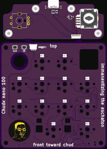
22 files in gerbs/
skills/footprint/SKILL.md · 25 lines · 2.6 KB
description: Generate compliant KiCad footprints from official KiCad Library Tools
skills/gerbers/SKILL.md · 18 lines · 0.9 KB
description: Generate, render, and visually review KiCad Gerber layers as a fabrication-output inspection step.
- pygerber gerber convert
skills/layout/SKILL.md · 23 lines · 4.3 KB
description: Place components and route KiCad PCB layouts with footprint checks, schematic pin swaps, and signal integrity best practices.
- ## Editing the active board in place
skills/layout-placement/SKILL.md · 344 lines · 21.5 KB
description: Place components on a KiCad board so each part sits where its circuit needs it, placement DRC passes, and every pad stays reachable, with IPC scripts that move parts and measure distances and routability. Covers reading the circuit, fixed parts, IC orientation, and decoupling, regulator, clock, RF and filter parts. Use for component placement; not for routing or schematic design.
- ## Save progress to the configured board
- ## Why parts go where they go
- ## 1. Read the circuit before moving anything
- ## 2. Fix the immovable, then orient the ICs
- ## 3. Place in order of how little distance each connection tolerates
- ## 4. Keep every pad reachable
- ## 5. Check, look, fix
- ## What the checks assume
- ## Working with the board
- PROVENANCE.md
- requirements.in
- requirements.txt
- scripts/grid_router.py
- scripts/group_search.py
- scripts/ipc_board.py
- scripts/local_search.py
- scripts/move.py
- scripts/pin_sides.py
- scripts/placement_audit.py
- scripts/route_check.py
- scripts/rules.py
- scripts/run.sh
- scripts/sidecar.py
STM32N657_SoM/build/
图表:C48-placement-search.log (scripts/local_search.py)
        230 legal candidates for C48 at U1.D1 (current gap 2.925 mm)
blocks  gap_mm  partner_mm   x        y       rot  faces  blocked pins
     0   2.867      9.000    97.600   95.050   90  True   []
     0   2.868      9.000    97.850   95.050   90  True   []
     0   2.884      9.000    98.100   95.050   90  True   []
     0   3.067      9.000    98.100   95.300    0  True   []
     0   3.069      9.000    98.350   95.300    0  True   []
skills/panelize/SKILL.md · 90 lines · 3.4 KB
description: Use KiKit to panelize a given PCB
- ## Preferred starting values
- ## KiKit behavior
- ## Useful commands
- kikit panelize
- kicad-cli pcb render
skills/pcb/SKILL.md · 32 lines · 2.5 KB
description: Review KiCad PCB layouts with DRC, layer renders, and 3D-model interference inspection.
- ## Editing the active board in place
- ## Placement
skills/pcb-product-render/SKILL.md · 53 lines · 5.0 KB
description: Create realistic Blender product renders from KiCad PCB projects, including refreshed 3D exports, physically plausible PCB materials, camera/stage setup, and visual validation.
- ## Required workflow
- ## Material targets
- ## Camera and stage
- ## Handoff requirements
skills/schematic/SKILL.md · 102 lines · 11.1 KB
description: Create, modify, and review KiCad schematics from selected parts, datasheets, reference designs, renders, and netlists.
- ## For Humans
- ## For Agents
- ### Save work in place
- ### How to draw the schematic
- ### How to do research
skills/symbol/SKILL.md · 19 lines · 1.9 KB
description: Generate compliant KiCad symbols